- 您现在的位置:买卖IC网 > Sheet目录483 > NDF08N50ZG (ON Semiconductor)MOSFET N-CH 500V 8.5A TO-220FP
NDF08N50Z
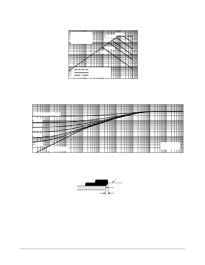
TYPICAL CHARACTERISTICS
100
10
V GS v 30 V
SINGLE PULSE
T C = 25 ° C
100 m s
1 ms
10 m s
10 ms
1
0.1
dc
R DS(on) LIMIT
THERMAL LIMIT
0.01
0.1
PACKAGE LIMIT
1 10 100
1000
V DS , DRAIN ? TO ? SOURCE VOLTAGE (V)
Figure 12. Maximum Rated Forward Biased
Safe Operating Area NDF08N50Z
10
50% (DUTY CYCLE)
1
0.1
20%
10%
5.0%
2.0%
0.01
1.0%
SINGLE PULSE
R q JC = 3.6 ° C/W
Steady State
0.000001
0.00001
0.0001
0.001
0.01
0.1
1.0
10
100
1000
PULSE TIME (s)
Figure 13. Thermal Impedance (Junction ? to ? Case) for NDF08N50Z
LEADS
HEATSINK
0.110 ″ MIN
Figure 14. Isolation Test Diagram
Measurement made between leads and heatsink with all leads shorted together.
*For additional mounting information, please download the ON Semiconductor
Soldering and Mounting Techniques Reference Manual, SOLDERRM/D.
http://onsemi.com
5
发布紧急采购,3分钟左右您将得到回复。
相关PDF资料
NDF08N50ZH
MOSFET N CH 500V 8.5A TO220FP
NDF08N60ZG
MOSFET N-CH 600V 7.5A TO220FP
NDF08N60ZH
MOSFET N-CH 600V 7.5A TO-220FP
NDF10N62ZG
MOSFET N-CH 620V .75OHM TO220FP
NDF11N50ZG
MOSFET N-CH 500V 12A TO-220FP
NDF11N50ZH
MOSFET N CH 500V 12A TO220FP
NDFEB 6X10MM
MAGNET PERM NDFEB 6.0X10.0MM
NDP6020P
MOSFET P-CH 20V 24A TO-220
相关代理商/技术参数
NDF08N50ZH
功能描述:MOSFET NFET 500V 7.5A RoHS:否 制造商:STMicroelectronics 晶体管极性:N-Channel 汲极/源极击穿电压:650 V 闸/源击穿电压:25 V 漏极连续电流:130 A 电阻汲极/源极 RDS(导通):0.014 Ohms 配置:Single 最大工作温度: 安装风格:Through Hole 封装 / 箱体:Max247 封装:Tube
NDF08N60Z
制造商:ONSEMI 制造商全称:ON Semiconductor 功能描述:N-Channel Power MOSFET 600 V, 0.95 ?
NDF08N60ZG
功能描述:MOSFET 600V 0.95 OHM TO- 220FP RoHS:否 制造商:STMicroelectronics 晶体管极性:N-Channel 汲极/源极击穿电压:650 V 闸/源击穿电压:25 V 漏极连续电流:130 A 电阻汲极/源极 RDS(导通):0.014 Ohms 配置:Single 最大工作温度: 安装风格:Through Hole 封装 / 箱体:Max247 封装:Tube
NDF08N60ZH
功能描述:MOSFET NFET 600V 7.5A RoHS:否 制造商:STMicroelectronics 晶体管极性:N-Channel 汲极/源极击穿电压:650 V 闸/源击穿电压:25 V 漏极连续电流:130 A 电阻汲极/源极 RDS(导通):0.014 Ohms 配置:Single 最大工作温度: 安装风格:Through Hole 封装 / 箱体:Max247 封装:Tube
NDF10N60Z
制造商:ONSEMI 制造商全称:ON Semiconductor 功能描述:N-Channel Power MOSFET 0.65 ?, 600 Volts
NDF10N60ZG
功能描述:MOSFET NFET T0220FP 600V 10A .65 RoHS:否 制造商:STMicroelectronics 晶体管极性:N-Channel 汲极/源极击穿电压:650 V 闸/源击穿电压:25 V 漏极连续电流:130 A 电阻汲极/源极 RDS(导通):0.014 Ohms 配置:Single 最大工作温度: 安装风格:Through Hole 封装 / 箱体:Max247 封装:Tube
NDF10N60ZH
功能描述:MOSFET NFET 600V 10A RoHS:否 制造商:STMicroelectronics 晶体管极性:N-Channel 汲极/源极击穿电压:650 V 闸/源击穿电压:25 V 漏极连续电流:130 A 电阻汲极/源极 RDS(导通):0.014 Ohms 配置:Single 最大工作温度: 安装风格:Through Hole 封装 / 箱体:Max247 封装:Tube
NDF10N62Z
制造商:ONSEMI 制造商全称:ON Semiconductor 功能描述:N-Channel Power MOSFET 620 V, 0.65 ?
